Samsung Electronics, a international chief in advanced semiconductor generation, today announced that it has advanced the industry’s first 12-layer 3-d-TSV (Through Silicon Via) generation.
Samsung’s new innovation is considered one of the maximum hard packaging technology for mass manufacturing of high-performance chips, because it requires pinpoint accuracy to vertically interconnect 12 DRAM chips thru a 3-dimensional configuration of more than 60,000 TSV holes, every of that is one-20th the thickness of a single strand of human hair.
Read More :- Logitech Enables Advanced Users to Achieve Peak Performance with MXMaster 3 and MX Keys
- ASUS Republic of Gamers Introduces New 300Hz Gaming Laptops at IFABerlin
- AMD Announces Worldwide Availability of AMD Ryzen™ PRO 3000 SeriesProcessors Designed to Power the Modern Business PC
- BIOSTAR Launches the NEW S120 Series Ultra Slim SSDs
- Nvidia GeForce v436.30 WHQL Released
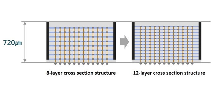
The thickness of the package deal (720㎛) stays similar to present day 8-layer High Bandwidth Memory-2 (HBM2) merchandise, that is a massive development in issue layout. This will help clients launch subsequent-era, high-capacity merchandise with higher performance capability while not having to change their gadget configuration designs.
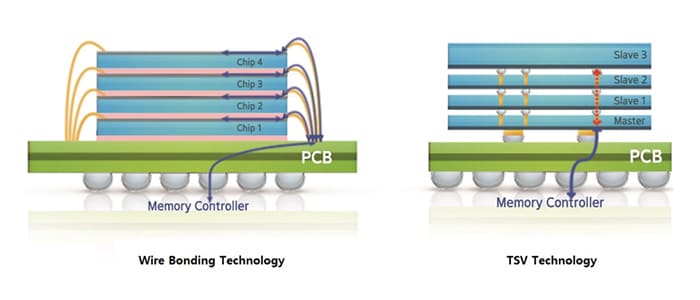
In addition, the 3-d packaging era additionally capabilities a shorter records transmission time among chips than the presently current cord bonding generation, ensuing in considerably faster velocity and decrease electricity consumption.
“Packaging technology that secures all of the intricacies of extremely-performance reminiscence is becoming exceptionally essential, with the huge range of recent-age packages, consisting of artificial intelligence (AI) and High Power Computing (HPC),” said Hong-Joo Baek, government vp of TSP (Test & System Package) at Samsung Electronics.
“As Moore’s law scaling reaches its limit, the function of three-D-TSV technology is predicted to emerge as even extra important. We need to be at the vanguard of this trendy chip packaging technology.”
Relying on its 12-layer 3D-TSV technology, Samsung will offer the best DRAM performance for applications which are facts-in depth and extremely high-pace.
Also, through growing the number of stacked layers from eight to 12, Samsung will quickly be capable of mass produce 24-gigabyte (GB)* High Bandwidth Memory, which gives three times the ability of 8GB high bandwidth reminiscence in the marketplace these days.
Samsung might be able to meet the swiftly developing market call for for excessive-ability HBM answers with its modern 12-layer 3D TSV era and it hopes to solidify its management in the top class semiconductor market.
*8GB mass-production product= 8Gb x 8 layers, 24GB developed product= 16Gb x 12 layers
*PKG go segment shape
*Wire bonding vs TSV technology